 CHIP
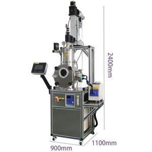
Single Crystal Pulling Furnace (CZ)
Czochralski furnace growing monocrystalline silicon ingots for wafer starting material.
- CZ pull, 6–12 in class
- Argon / vacuum chamber
- Diameter and resistivity on request
Wafer & chip tools
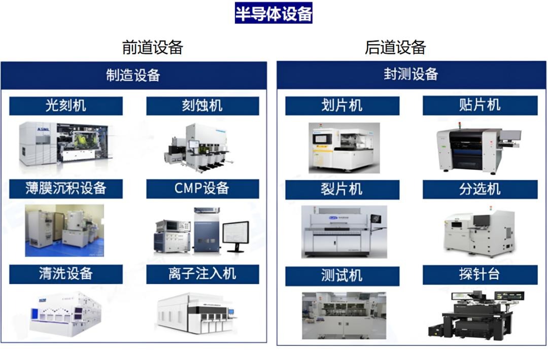
CZ furnaces, lithography, PVD, lapping and plasma etch for front-end chip work. Quoted against wafer diameter and process node.
Catalogue
CZ furnaces, lithography, PVD, lapping and plasma etch for front-end chip work. Quoted against wafer diameter and process node.
CHIPCzochralski furnace growing monocrystalline silicon ingots for wafer starting material.
 CHIP
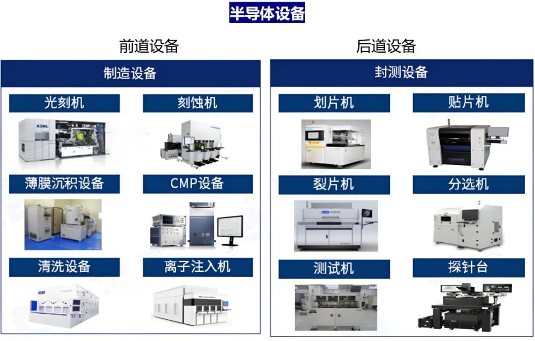
Grouped core tools for front-end wafer lines: clean handling, process modules and metrology interfaces.
 CHIP
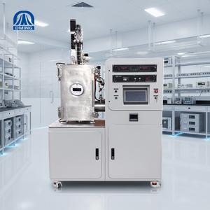
Magnetron sputter tool depositing metal and barrier films on wafers.
 CHIP
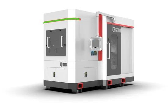
Multi-wire saw slicing CZ ingots into wafers with controlled thickness and TTV.
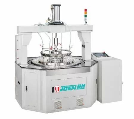 CHIP
Double-side lapping and CMP-style polish to bring sliced wafers to spec thickness and roughness.
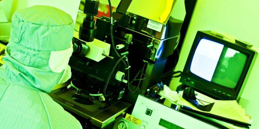 CHIP
Stepper / scanner exposing wafer resist with DUV or EUV optics for critical layers.
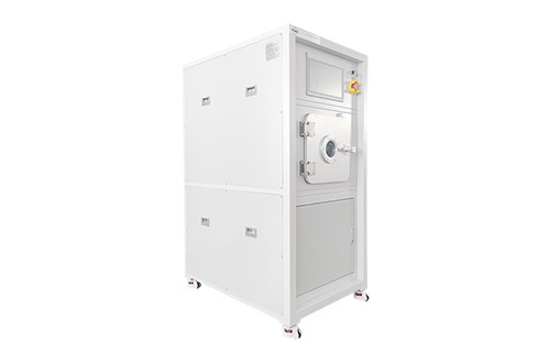 CHIP
Dry plasma etch for dielectric and metal layers with anisotropic profiles.
Capabilities
CZ, wire saw and polish quoted to ingot and wafer diameter.
Lithography, PVD and plasma etch to process node.
Factory acceptance and English operating files.
Crate packing for precision tools.
Facility
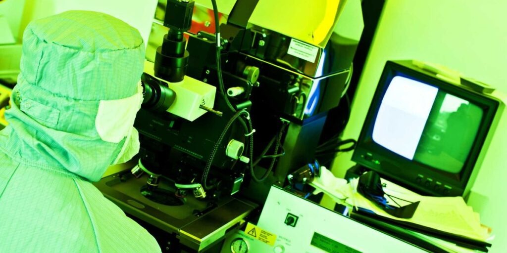
Wafer tools prepared for FAT.
Send drawings or process windows. The team replies within one business day.
Quality
Utility drawings and FAT records travel with the tool.
HANDOVER
Request a quotation
Wafer diameter, node and destination. Reply within one business day.